Global semiconductor makers are increasingly shifting their focus eastwards, expanding their operations in Japan. These companies are scaling up production and forging partnerships with local firms for research and development.
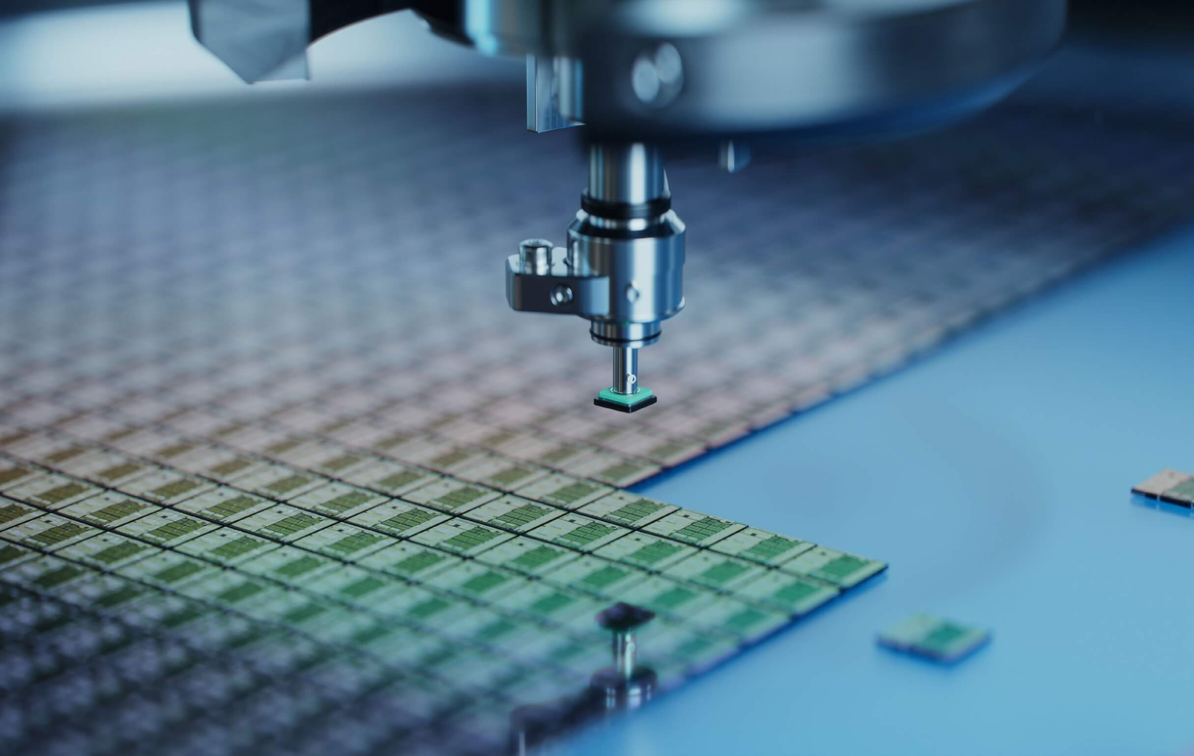
A key area of collaboration is advanced packaging, a set of innovative techniques that integrate semiconductor chips into their final form. As chip miniaturisation approaches its physical limits, manufacturers are turning to advanced packaging methods to improve efficiency by closely integrating multiple chips. This approach is crucial to meeting the growing demands of rapidly evolving applications like artificial intelligence.
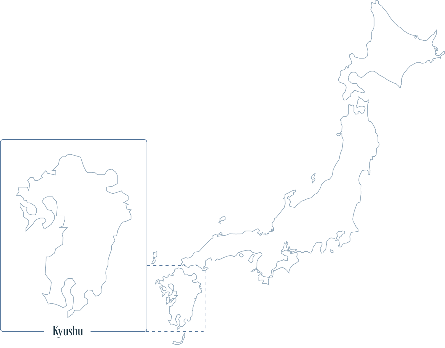
Japan is at the forefront of this technological frontier. Over the past year, Taiwanese semiconductor giant TSMC has not only announced plans to build a second plant in Kumamoto for producing 6-nanometre chips but also established an advanced packaging R&D centre in Ibaraki.
Meanwhile, US-based Intel is partnering with 14 Japanese companies to develop technologies that automate back-end semiconductor manufacturing processes, including advanced packaging. South Korea’s Samsung is also bolstering its presence in Japan, expanding its Yokohama facility to advance research in packaging technologies.
Foreign investments in Japan’s semiconductor industry
Chipmakers
Domestic Suppliers
Company: Rapidus
Investment: $33 billion*
Company: Kioxia†/Western Digital (2024)
Investment: $4.9 billion (combined)
Company: Samsung
Investment: $280 billion
Company: Kioxia†/Western Digital (2024)
Investment: $4.9 billion (combined)
Company: Micron
Investment: $3.7 billion
Company: TSMC
Investment: $20 billion**
Company: Sony
Investment: Undisclosed
Company: Sony
Investment: Undisclosed


| Company | Investment | |
|---|---|---|
| 1 | Rapidus | $33 billion* |
| 6 | TSMC | $20 billion** |
| 7 8 | Sony | Undisclosed |
| 2 4 | Kioxia†/Western Digital (2024) | $4.9 billion (combined) |
| 5 | Micron | $3.7 billion |
| 3 | Samsung | $280 billion |
*Estimate for mass production
**Total for two plants
† Kioxia is a Japanese company; joint venture with the U.S.’s Western Digital
†† Research and development facility
Source: Complied by Nikkei Asia based on government and company announcements.
Vital ecology for the semiconductor industry
Several factors are drawing these chip giants to Japan: geopolitical risks, trade restrictions with China, a weaker yen and substantial subsidies from the Japanese government. The push for increased local production is also a driver, with Japanese startup Rapidus ambitiously constructing a plant aimed at mass-producing chips with a 2-nanometre circuit width by 2027.
Japan provides a uniquely attractive ecosystem for high-end chip makers, further fuelling this growing interest.
Geopolitical risks, trade restrictions with China, a weaker yen and substantial Japanese government subsidies are drawing these chip giants [into Japan].
“Unlike their chipmaking counterparts, Japanese semiconductor materials and manufacturing equipment makers have continued to maintain their global market share of some 30 to 50 per cent since the 1990s,” explains Nobuyuki Suzuki, president of Electronics Company at AGC, a leading supplier of advanced materials for top chip makers.
AGC is one of three companies worldwide that supply photomask blanks for EUV lithography, a highly specialised technology that semiconductor manufacturers use to produce the most advanced chips. (Photomasks are essentially templates that guide the patterning of circuits onto semiconductor wafers, which are used to produce microchips.)
AGC is also a market leader in high-end slurries, crucial to the chip manufacturing process. The company is also pioneering glass-core substrates, poised to drive the next phase of advanced packaging technology.
Japan dominates key elements of global chip supply chain
Photoresist data as of 2020, all other data as of 2021
Japanese companies’ combined global market share per sector
Source: Complied by Nikkei Asia based on report by Japanese government and NTT Advanced Technology Corporation
AGC is a key player in the ongoing AI revolution, contributing to the development of the advanced chips that drive it.
AGC entered the semiconductor industry in the mid-1980s, supplying synthetic quartz for traditional lithography and ceramic components for chip production. In 2003, the company joined an international consortium of firms dedicated to advancing EUV lithography. Recognising this opportunity, the company decided to not only supply quartz but also to produce the photomask blanks themselves.

Glass is indispensable for next-generation chips
An EUV mask blank is a glass substrate coated with optical films on both sides. The technical requirements for these blanks are incredibly stringent, demanding near-zero thermal expansion, perfectly smooth and flat surfaces, and absolutely no particulate contamination of the glass surface or optical coatings. To put this into perspective, the standard for contamination is equivalent to having no pollen over an entire football pitch. AGC invested more than a decade in meeting these exacting requirements.
“We knew how difficult it would be to manufacture EUV mask blanks with these qualities. AGC is the only supplier in the world that takes care of all essential materials and processes required to fabricate the EUV mask blank. We knew we could count on our expertise in material and manufacturing processes,” says Suzuki.
AGC’s perseverance paid off, although it took time. Mass production of EUV mask blanks only began in 2017. Since then, sales have surged, increasing by 50 per cent year on year last year, with projections for even faster growth in 2024, potentially reaching ¥40bn ($272m). The company anticipates double-digit growth in the coming years.
AGC’s EUV photomask blanks sales
Source: AGC
EUV mask blanks continue to be customised for each new generation of semiconductor chips, preventing their commodification. The industry has extremely high entry barriers, due to the technical expertise and capital investment required and because customers are reluctant to switch suppliers. This is similarly true for slurries, used to polish high-end wafers, where AGC is a market leader in ceria-based solutions. Ceria is a rare earth metal oxide that can selectively polish certain materials, making it particularly valuable in the semiconductor industry.
AGC also plays a pivotal role in developing glass-based technologies for advanced packaging. Currently, packages are made by mounting chiplets—integrated circuits optimised for specific functions and assembled into more complex systems—onto organic substrates and polymer films. However, as these packages grow larger and more sophisticated, organic substrates become less suitable.
“Unlike organic substrates, glass is flatter, smoother, more solid, resilient to heat and warpage, and fine-pitch holes at very high precision can be formed,” explains Suzuki. “Glass is one of the promising options for providing the core of advanced packaging. We have been researching and developing solutions for this for the past decade.”
Suzuki also suggests that other crucial parts of chip packaging, such as the interposers that facilitate communication between chips, are also likely to perform better when made of glass, particularly in structures with very high-density interconnects.
Smaller chips, larger packages
Semiconductor manufacturing is typically divided into two stages: the front-end process, which concentrates on wafer fabrication, and the back end, which deals with assembling the integrated circuit.
AGC is making significant contributions to both the front end, by enabling smaller integrated circuits through its EUV mask blanks and slurries, and the back end, by facilitating the assembly of these circuits into larger, more advanced packages.
Japanese glass will be central to the future of semiconductor innovation. It will enable the creation of ever-smaller, next-generation chips within increasingly complex packages, driving new levels of computing power.


